Table of Contents
1. The Strategic Value of a One-Stop PCB and PCBA Solution
2. Bridging the DFM Gap: Engineering Beyond Connectivity
3. Component Obsolescence and Lifecycle Management
4. Quality Control Metrics in a One-Stop PCB and PCBA Solution
5. Scaling from Prototype to Mass Production
1. The Strategic Value of a One-Stop PCB and PCBA Solution
In the rapidly evolving electronics market, speed-to-market is no longer just an advantage-it is a survival requirement. For OEMs and hardware startups, managing multiple vendors for fabrication, component sourcing, and assembly often leads to communication silos and costly delays. A integrated one-stop PCB and PCBA solution eliminates these friction points by consolidating the entire lifecycle under a single technical roof.
While many providers claim to offer end-to-end services, true excellence in a one-stop PCB and PCBA solution lies in the depth of technical oversight provided during the transition from Gerber files to a functional, populated board. This involves managing complex material interactions and ensuring supply chain resilience.
Traditional fragmented manufacturing often results in "finger-pointing" when defects occur. A one-stop PCB and PCBA solution provides a single point of accountability. This synergy allows for parallel processing: component procurement begins the moment the PCB design is finalized, reducing total lead times by up to 30%.
Technical Insight: Fragmentation typically adds 7-14 days to the development cycle due to shipping between facilities and re-incoming quality control (IQC) at each stage.
2. Bridging the DFM Gap: Engineering Beyond Connectivity
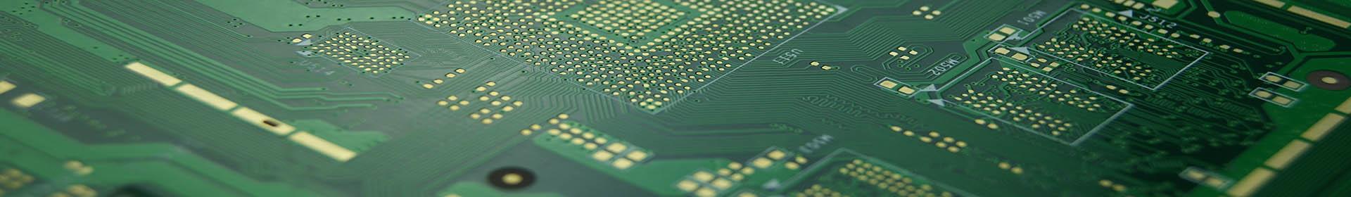
2.1 Advanced HDI and High-Speed Signal Integrity
Modern high-speed designs (e.g., 5G, AI, IoT) require more than just standard routing. A high-tier one-stop PCB and PCBA solution analyzes the stackup for DK (Dielectric Constant) and DF (Dissipation Factor) consistency across the board. Failure to manage these can lead to impedance mismatches of >10%, rendering high-speed signals unstable.
2.1.1 Via-in-Pad and Microvia Reliability
In HDI designs, using Via-in-Pad technology requires precision resin plugging and flat capping. In our one-stop PCB and PCBA solution, we ensure that the surface flatness of the capped via is within +/- 5μm, preventing solder paste "voiding" during the assembly phase.
3. Component Obsolescence and Lifecycle Management
One critical area often missing from standard service descriptions is proactive component management. A robust one-stop PCB and PCBA solution doesn't just buy what’s on the BOM; it analyzes the lifecycle of every part.
Statistical Reality: Approximately 15% of components on a typical industrial BOM face "End of Life" (EOL) or long lead times (>26 weeks) within 12 months of product launch.
3.1 Strategic Sourcing and Risk Mitigation
Our one-stop PCB and PCBA solution utilizes real-time API integrations with global distributors (Mouser, Digikey, Arrow) to identify EOL risks during the DFM stage. This allows engineers to suggest drop-in replacements or footprint modifications before the first board is even fabricated.
4. Quality Control Metrics in a One-Stop PCB and PCBA Solution
4.1 First Pass Yield (FPY) Targets
While competitors focus on "Low Price," we focus on First Pass Yield. In a sophisticated one-stop PCB and PCBA solution, FPY for complex PCBA should exceed 98.5%. This is achieved through automated optical inspection (AOI), X-ray for BGA components, and ICT (In-Circuit Testing).
Test Method Focus Area Typical Fault Detection Rate
3D AOI Solder fillets, polarity, missing parts >99% of visible defects
AXI (X-Ray) BGA/QFN solder bridging, voids Detects internal solder voids >15%
Functional Test (FCT) Full system logic and power-on Ensures 100% field readiness
5. Scaling from Prototype to Mass Production
Transitioning from a 5-unit prototype run to 5,000-unit mass production is where many designs fail. A one-stop PCB and PCBA solution ensures that the panelization and stencil design used in prototyping are optimized for high-speed pick-and-place machines from day one.
5.1 Traceability and Compliance
For medical and automotive clients, traceability is non-negotiable. Our one-stop PCB and PCBA solution includes component-level traceability, recording the batch numbers and date codes of every passive and active component used in your build, compliant with IPC-Class 2 and Class 3 standards.
About Author
David Chen https://www.linkedin.com/in/pcbcoming/
David Chen boasts an extensive professional background in PCBA manufacturing, PCBA testing, and PCBA optimization, with specialized expertise in high-precision PCBA fault analysis and rigorous PCBA reliability testing. Skilled in complex circuit design and cutting-edge advanced PCB manufacturing processes, he delivers solutions that elevate product durability and performance across industrial applications. His technical articles focusing on PCBA manufacturing workflows and testing methodologies are widely cited by industry peers, research institutions, and technical platforms, solidifying his reputation as a recognized technical authority in the global circuit board manufacturing sector.