

In today's fast-paced electronics market, bringing a product from concept to reality requires a seamless, highly efficient, and technologically rigorous manufacturing process
1. Technical Depth in One-Stop Engineering Services
A premium one-stop PCBA provider does not merely execute manufacturing; they act as an elite engineering partner from the earliest stages of design review through complex production.
Advanced Design for Manufacturing (DFM) & Design for Testing (DFT)
Before a single component is sourced, a comprehensive DFM and DFT review is critical to bridge the gap between theoretical design and physical yield.
-
DFM Layout Optimization: Reviewing trace widths, spacing, and via structures to prevent manufacturing defects. Specialized focus is placed on avoiding acid traps (acute angles in copper traces that trap etching chemicals) and optimizing thermal reliefs to prevent heat sinking during soldering.
-
Aspect Ratio Validation: Ensuring the aspect ratio (drill depth to hole diameter) for microvias does not exceed industry thresholds (typically 10:1 for standard through-holes and 1:1 for blind or buried microvias) to guarantee reliable copper plating.
-
Solder Mask & Silk Screen Check: Verifying proper solder mask dams (minimum 4 mils) between fine-pitch pads to completely eliminate the risk of solder bridging.
-
DFT Implementation: Incorporating dedicated test points into the schematic and layout, ensuring a minimum distance (typically 50 to 100 mils) between test points to facilitate seamless Automated Test Equipment (ATE) and bed-of-nails fixture placement.
Component Sourcing and Lifecycle Management
Global component sourcing is integrated into the engineering workflow rather than treated as a pure purchasing function. One-stop providers leverage real-time API integrations with global distributors to monitor Lifecycle Statuses (such as Active, Not Recommended for New Designs (NRND), or End of Life (EOL)). When an EOL component is detected, engineers immediately provide pin-to-pin compatible alternatives or cross-references, eliminating design dead-ends before production begins.
2. Critical Manufacturing Parameters and Precision Capabilities
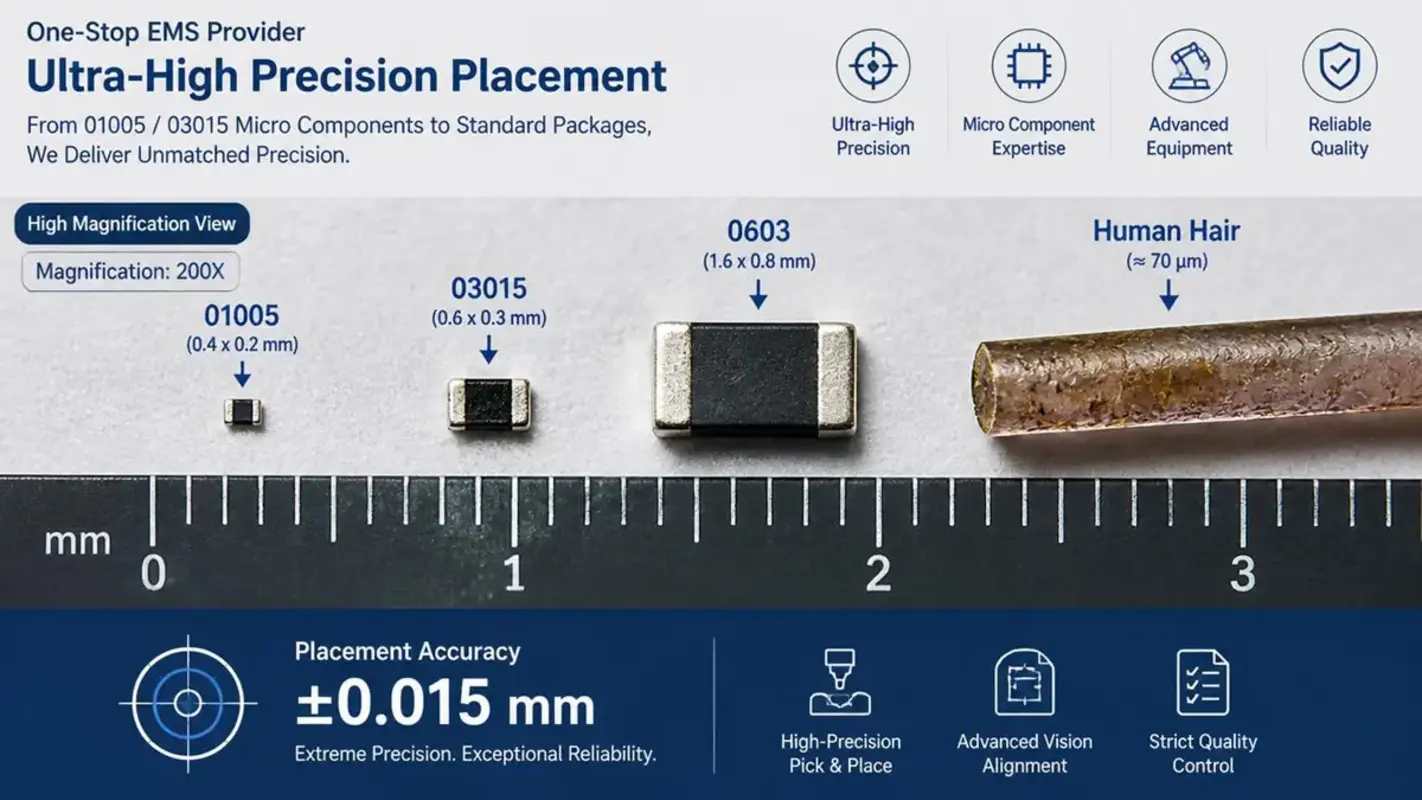
Micro-component size comparison (01005 vs 0603) and $\pm0.015\text{ mm}$ high-precision SMT placement capabilities.
To handle modern, high-density electronic designs, a one-stop partner must possess high-precision manufacturing capabilities that can be quantified through rigorous technical specifications.
-
Minimum Component Size: 0402, 0201 packages (Standard) | 01005, 03015 micro-components, and ultra-fine pitch WLCSP (Advanced)
-
BGA and QFN Pitch: Greater than or equal to 0.5 mm pitch (Standard) | Down to 0.35 mm pitch with micro-BGA alignment (Advanced)
-
Placement Accuracy: Plus/minus 0.05 mm (Standard) | Plus/minus 0.015 mm at 3-sigma for ultra-fine pitch components (Advanced)
-
Max PCB Layer Count: 2 to 8 layers (Standard) | Up to 32+ layers, including High-Density Interconnect / HDI (Advanced)
-
Surface Finish Options: HASL, Lead-Free HASL (Standard) | ENIG, ENEPIG, OSP, Immersion Silver/Tin (Advanced)
-
Board Thickness Range: 1.6 mm Standard thickness (Standard) | 0.2 mm Ultra-thin to 6.0 mm Heavy copper / Backplane (Advanced)
Reflow Profile Control and Voiding Mitigation
Precision assembly relies heavily on advanced thermal management during the reflow process. High-end lines utilize multi-zone (10 zones or higher) lead-free reflow ovens with nitrogen (N2) atmospheres to minimize oxidation.
Engineers meticulously calibrate the reflow profile—managing the ramp-up rate (1 to 3 degrees Celsius per second), liquidus time (typically 60 to 90 seconds above 217 degrees Celsius for SAC305 alloy), and peak temperature (235 to 245 degrees Celsius). For critical components like bottom-termination BGAs and QFNs, vacuum reflow technology is employed to drive voiding rates below 10%, far exceeding the standard IPC threshold of 25%, thereby ensuring optimal thermal and electrical conductivity.
3. Application-Specific Tailoring and Case Studies
A one-stop PCBA approach is highly adaptable, adjusting its workflows and technical focus to meet the highly specialized demands of different vertical markets.
Medical Electronics: Ultra-Low Noise & High Traceability
-
The Challenge: A medical device startup required a multi-channel patient monitoring system demanding ultra-low signal noise and 100% component traceability.
-
The Solution: The one-stop partner optimized the layer stackup using advanced HDI blind-via technology to isolate sensitive analog sensor traces from high-speed digital switching lines.
-
The Outcome: Implementing automated component barcode tracking coupled with laser-marked 2D data-matrix codes on each PCB ensured full component-to-board traceability, reducing electromagnetic interference (EMI) by 22dB and accelerating FDA compliance approval.
Automotive Electronics: Thermal Management & High Vibrations
-
The Challenge: An automotive client needed an Under-the-Hood Electronic Control Unit (ECU) capable of withstanding extreme thermal cycles and constant mechanical vibration.
-
The Solution: The provider recommended a heavy-copper PCB substrate (3 oz copper thickness) and integrated aluminum-core thermal pads. During assembly, high-temperature melting alloys were coupled with an automated selective conformal coating process (silicone-based, 50-micrometer thickness).
-
The Outcome: The coating provided robust insulation against moisture, dust, and automotive fluids, while the specialized alloy prevented solder joint fatigue during mechanical stress testing.
4. Uncompromising Reliability, Testing, and Global Compliance
End-to-end visibility allows providers to implement stringent quality control and inspection mechanisms at every single step of the production chain.
The Standard Quality Workflow:
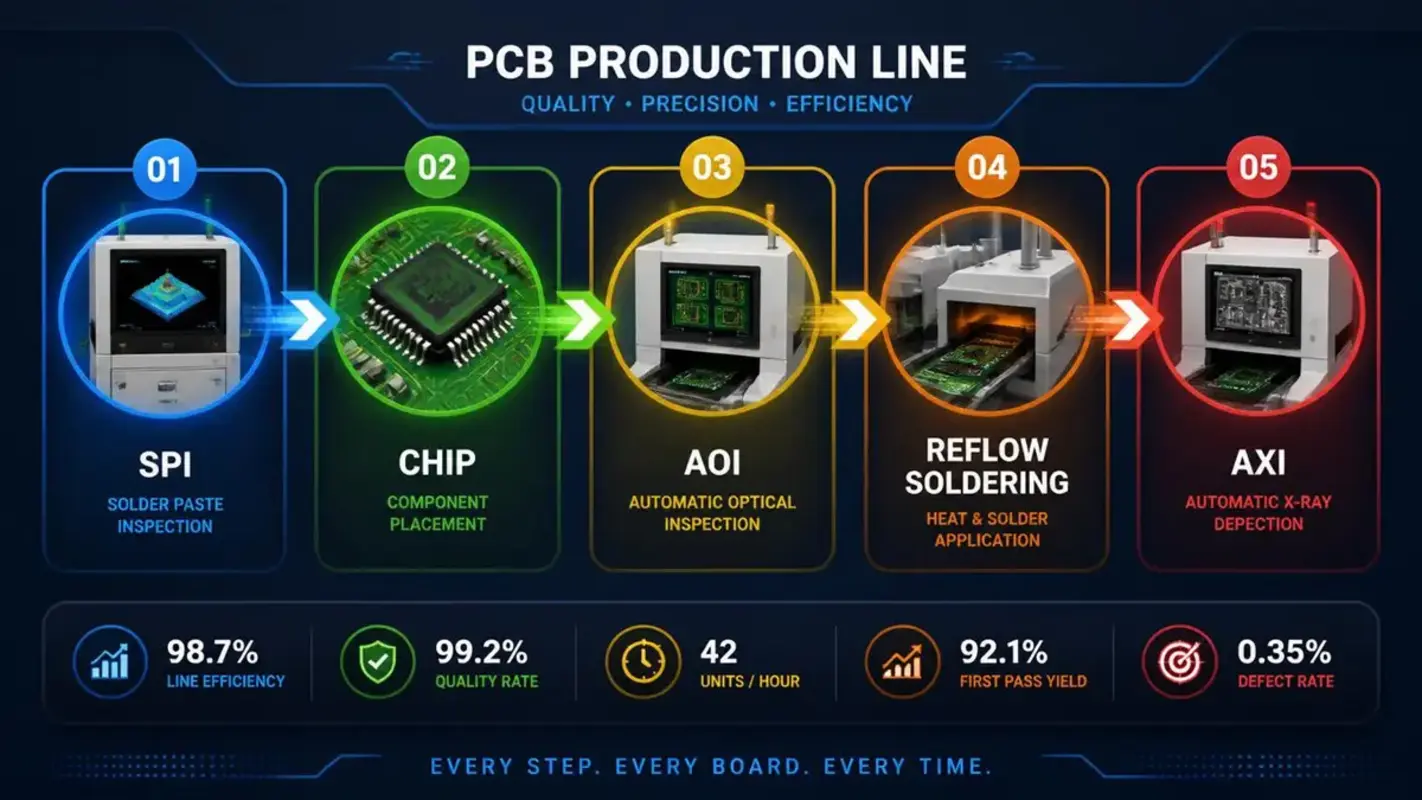
Seamless PCBA production line workflow exhibiting 5-step automated quality control from SPI to AXI.
-
Incoming Material: Component Inspection and Solder Paste Inspection (SPI)
-
SMT Assembly: High-Speed SMT Component Placement
-
Reflow Stage: Pre-Reflow AOI -> Reflow Soldering (Vacuum / N2) -> Post-Reflow AOI
-
Deep Inspection: Advanced Testing (3D X-Ray / AXI, ICT, and Functional Testing)
-
Final Output: Box-Build Assembly and Compliance Packaging
The Multi-Tiered Inspection Ecosystem
-
3D Solder Paste Inspection (SPI): Deployed immediately after stencil printing to analyze solder paste volume, area, and height profile, capturing 70% of potential soldering defects before component placement.
-
Automated Optical Inspection (AOI): Utilized both pre-reflow and post-reflow to verify component presence, orientation (polarity), shifting, and solder joint fillets.
-
Automated X-Ray Inspection (AXI): Vital for hidden solder joints. 3D X-ray laminography inspects the interior of BGA balls and QFN pads to detect hidden bridges, insufficient wetting, or internal voiding.
-
In-Circuit Testing (ICT) & Flying Probe: Evaluates component values, opens, shorts, and basic electrical functionality across the entire circuit matrix.
-
Functional Testing (FCT) & Burn-In Testing: Simulates the final operating environment by applying full working voltages and data inputs. Thermal burn-in testing (e.g., 48 hours at 60 degrees Celsius) accelerates potential early-life component failures, ensuring that only rock-solid, market-ready products are shipped.
International Standards and Regulatory Compliance
A reputable one-stop manufacturing facility maintains a robust framework of globally recognized certifications, ensuring products meet international legal and safety benchmarks:
-
ISO 9001:2015: Quality management systems ensuring consistent product and service standards.
-
IATF 16949: Strict quality management requirements specifically for the automotive supply chain.
-
ISO 13485: Comprehensive quality management system requirements for the design and manufacture of medical devices.
-
IPC-A-610 Class 2 & Class 3: Strict adherence to acceptability of electronic assemblies. Class 3 standards are rigorously applied to aerospace, medical, and military hardware where downtime is not an option.
-
RoHS / REACH Compliant: 100% lead-free and hazardous-substance-free material procurement and manufacturing lines, fulfilling European and global environmental mandates.
Conclusion
The strategic advantage of an integrated, one-stop PCB assembly workflow is clear: it eliminates fragmented communication, drastically accelerates time-to-market, and reduces logistical overhead. However, the true differentiator lies in engineering execution.
By embedding deep DFM/DFT analysis, maintaining high-precision manufacturing metrics, tailoring processes to specific industry applications, and enforcing rigorous compliance and multi-tiered testing, a top-tier one-stop provider does more than just assemble parts. They mitigate risk, protect intellectual property, optimize overall material costs, and empower businesses to dedicate their resources entirely to innovation and scalability. For any company striving to deploy next-generation electronics efficiently, a technically robust one-stop PCBA partner is the foundational cornerstone of a successful product launch