When developing advanced RF, microwave, or high-speed digital electronics, knowing the typical high frequency PCB turnaround time for prototype orders is critical for meeting tight project milestones. For hardware engineers and procurement managers operating in the middle and bottom of the sales funnel (MOFU/BOFU), lead time is often just as vital as electrical performance. Understanding how material selection, layer count, and manufacturing complexities influence this timeline can mean the difference between a successful product launch and a missed market window.
Understanding High-Frequency PCB Lead Times
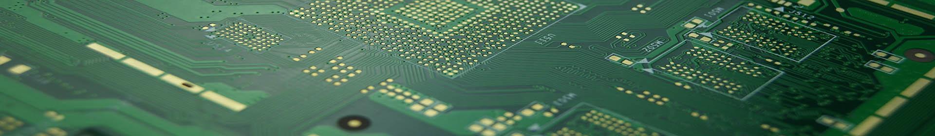
High-frequency printed circuit boards (PCBs)—typically operating in the 500 MHz to 100 GHz+ range—require specialized materials like Rogers, Taconic, or Isola, alongside highly precise manufacturing tolerances. Because of these stringent requirements, the high frequency PCB turnaround time for prototype orders is inherently different from standard FR-4 boards.
Standard vs. High-Frequency Prototype Timelines
For a standard FR-4 prototype, a quick-turn shop can easily spin a board in 24 to 48 hours. However, high-frequency laminates behave differently under mechanical drilling, laser ablation, and chemical plating, which extends the fabrication schedule.
Definition: Turnaround Time (TAT)
In high-frequency prototyping, TAT represents the total clock hours or business days from the moment the design files (Gerber/ODB++) pass the manufacturer’s Design for Manufacturing (DFM) review to the moment the finished boards ship out.
High Frequency PCB Turnaround Time Matrix
To help engineering teams estimate schedules and optimize budgeting during the BOFU purchasing stage, the matrix below outlines expected lead times based on design complexity and urgency tiers.
| Prototype Tier | Layer Count & Complexity | Quick-Turn Option | Standard Prototyping Lead Time |
|---|---|---|---|
| Basic HF Prototype | 2-Layer rigid, pure Rogers (e.g., RO4003C / RO4350B), standard surface finish (ENIG). | 48 – 72 Hours | 5 – 7 Business Days |
| Advanced HF / Hybrid | 4 to 8-Layer Hybrid stack-up (FR-4 combined with Rogers), controlled impedance testing. | 3 – 5 Business Days | 7 – 10 Business Days |
| Complex Multi-layer HF | 8+ Layers, blind/buried vias, microvias, sequential lamination, cavity designs. | 5 – 7 Business Days | 10 – 15 Business Days |
To put these timelines into perspective, consider a recent 2025 aerospace project executed by a leading defense tier-1 supplier. The engineering team needed a 6-layer hybrid prototype (Rogers RO4350B outer layers for RF signals, FR-4 inner layers for power/ground) for a 24 GHz radar sensor.
- The Challenge: The initial design layout failed the fabricator's initial automated DFM check due to insufficient trace-to-copper-pour spacing, risking a 48-hour delay.
- The Solution: By utilizing a dedicated prototype manufacturer offering real-time CAM engineering support, the files were corrected within 3 hours.
- The Result: The manufacturer achieved a high frequency PCB turnaround time for prototype orders of exactly 4 business days under a premium quick-turn agreement. The data showed tight impedance tolerances within ±5%, validating that speed does not have to compromise signal integrity.
What Factors Delay High Frequency PCB Prototyping?
When evaluating suppliers, buyers frequently ask critical long-tail MOFU/BOFU questions regarding what actually drives up lead times.
1. Material Availability and Lead Times
Unlike standard FR-4, which is always in stock, exotic high-frequency laminates (especially specialized PTFE-based substrates with specific dielectric constants like εr = 2.2 or 10.2) may require custom ordering. If a fabricator does not stock the exact material or copper weight required, the material acquisition alone can add 2 to 3 weeks to your timeline.
2. Complex Stack-ups and Hybrid Lamination
Are you designing a pure high-frequency board or a hybrid stack-up? Hybrid boards require balancing the different thermal expansion coefficients (CTE) of FR-4 and Rogers materials during the press cycle. Delamination prevention requires distinct temperature profiling, adding hours to the lamination phase.
3. Advanced Via Technologies
High-speed RF boards frequently employ blind vias, buried vias, or via-in-pad structures to minimize parasitic capacitance and inductance. Every sequential lamination and drilling cycle added to the workflow expands the overall high frequency PCB turnaround time for prototype orders.
[Standard Processing] -> DFM Approval -> Drilling -> Plating -> Etching -> Shipping (5 Days)
[Complex HF Processing] -> DFM Approval -> Laser Drill -> Lamination 1 -> Mechanical Drill -> Lamination 2 -> Specialized Etching -> Tighter QA -> Shipping (10+ Days)
FAQ: Optimizing Your Prototype Order for Faster Delivery
How can I get a 48-hour quick-turn on a high-frequency PCB prototype?
To secure the fastest possible high frequency PCB turnaround time for prototype orders, you must use pre-stocked materials (like Rogers 4000 series), provide flawless ODB++ files, keep the design to 2 or 4 layers without blind/buried vias, and pre-approve any minor DFM adjustments with your fabricator's engineering team.
Does controlled impedance testing extend the prototype lead time?
Yes, but minimally if planned correctly. Including an impedance coupon requires the manufacturer to run Time-Domain Reflectometry (TDR) testing. This adds roughly 4 to 12 hours to the final quality assurance phase but ensures the board meets your precise RF performance metrics before shipping.
Which surface finish is best for fast-turnaround RF prototypes?
Electroless Nickel Immersion Gold (ENIG) is highly recommended for both its excellent shelf life and its standardized processing time in most quick-turn facilities. For ultra-high frequencies where the skin effect makes nickel undesirable, Immersion Silver or ISIG can be used, though they may add 24 hours of processing time depending on the shop's daily line setups.
Conclusion: Balancing Speed, Cost, and Performance
Ultimately, the typical high frequency PCB turnaround time for prototype orders ranges from 3 to 10 business days, depending heavily on material readiness and stack-up complexity. When fast time-to-market is your primary objective, partnering with a manufacturer that maintains a robust inventory of specialized RF laminates and offers front-end DFM engineering support is paramount. By aligning your design constraints with the fabricator's in-stock capabilities early in the design phase, you can confidently compress your prototyping cycle and secure reliable high-frequency performance on the first spin.