1. Introduction
In modern electronic hardware architectures—particularly AI compute servers, multi-gigabit telecom arrays, and high-frequency edge platforms—traditional double-sided circuit designs have become completely inadequate. High-speed signaling requires tight electromagnetic confinement, structured power-distribution networks (PDN), and dense spatial routing topologies that only multilayer stacks can deliver. However, custom multilayer fabrication historically imposed steep entry barriers, with tooling setup fees often exceeding thousands of dollars per iteration.
Today, the industry faces an unprecedented surge in demand for cost-effective prototyping solutions. Hardware startups, specialized R&D divisions, and university research labs must operate under tight financial constraints while matching fast product development cycles. The core value proposition of a professional, budget-conscious multilayer prototyping vendor lies in resolving this exact tension: leveraging shared panel fabrication and optimized Design for Manufacturability (DFM) rulesets to deliver high-performance, multi-layered substrates at a fraction of standard commercial costs.
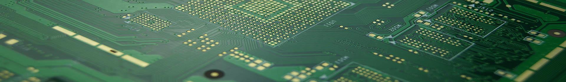
2. What Is a Multilayer PCB Prototype?
Unlike simple boards, a multilayer architecture utilizes internal routing environments to significantly expand trace routing capacity, simplify power distribution, and establish precise reference layers for high-speed signal pathways.
Typical Stack-Up Structures
| Layer Count | Standard Thickness | Common Stack-Up Configuration | Typical Substrate |
|---|---|---|---|
| 4 Layers | 1.6 mm (0.062") | L1: Signal (Top) / L2: Ground / L3: Power / L4: Signal (Bottom) | Standard FR-4 (Tg 135°C–140°C) |
| 6 Layers | 1.6 mm (0.062") | L1: Signal / L2: Ground / L3: Inner Signal / L4: Inner Signal / L5: Power / L6: Signal | Mid-Tg FR-4 (Tg 150°C) |
| 8 Layers | 1.6 mm / 2.0 mm | L1: Signal / L2: Ground / L3: Signal / L4: Ground / L5: Power / L6: Signal / L7: Ground / L8: Signal | High-Tg FR-4 (Tg 170°C–180°C) |
| 10+ Layers | 2.0 mm / 2.4 mm+ | Multi-power core sets, interleaved Ground shielding planes, and dual high-speed signal pairs | Ultra-low-loss Co-Polymers (Megtron 6, Rogers) |
Industry Applications & Scenario Localization
- AI Compute Clusters & Servers: High-layer-count backplanes (often 12 to 24 layers in production, prototyped in sub-sections) designed to handle massive, ultra-fast parallel computing throughput.
- Telecom Switching Platforms: 5G base station transceiver modules that demand high-frequency RF trace configurations.
- Medical Diagnostic Electronics: Multi-channel MRI/CT data acquisition boards requiring tight noise isolation to capture exceptionally weak analog input signals.
- Automotive ADAS Systems: High-reliability sensor integration modules running radar and vision-processing logic under volatile thermal conditions.
Key Design Features & Engineering Parameters
Managing advanced layouts requires operating within strict signal integrity parameters:
- Controlled Impedance: Crucial for suppressing signal reflections on critical tracks. Standard commercial tolerances are kept at ±10%, though advanced high-speed lines frequently require ±5% matching.
- High-Speed Routing: Routing protocols must comfortably support data transmission rates like 224G \; PAM4 or ultra-fast SerDes links, which are highly susceptible to skin effect losses and via stub reflections.
- EMI Suppression: Allocating dedicated internal copper layers as solid ground reference planes creates a highly effective Faraday shield, dropping both forward crosstalk and outward electromagnetic emissions.
3. Why Choose Cheap Multilayer PCB Prototype Services?
The primary driver behind budget prototyping is commercial viability during the earliest phases of development. If an engineering firm were forced to pay standard volume production tooling and setup surcharges just to test an early revision, the financial burn rate would rapidly drain venture capital or project allocations. Cheap prototype services eliminate this hurdle by spreading fixed manufacturing costs across multiple customers on a single production panel.
Prototyping vs. Mass Production Cost Dynamics
In low-volume prototyping, the cost structure is heavily dominated by engineering labor, front-end CAM data optimization, and initial machine alignment preparation. In contrast, mass production costs are primarily driven by continuous raw material volume consumption, chemical processing cycles, and overall panel yields. Budget prototype services capitalize on this difference by streamlining the front-end intake process via automated web portals, passing those engineering savings directly down to the customer.
In our factory lamination presses, running a custom 8-layer stack with non-standard prepreg thicknesses can tie up a multi-stage vacuum press for over 90 minutes per cycle. By standardizing our low-cost prototype lines on a fixed, symmetric stack-up using standard Isola or ShengYi FR-4, we can nest up to 12 completely different client designs on the exact same production panel. This maximizes our panelization efficiency and slashes the setup cost per customer by more than two-thirds.
4. Key Cost Drivers in Multilayer PCB Prototyping
To keep prototype budgets under tight control, engineers must carefully manage these five critical manufacturing cost drivers:
- Layer Count and Lamination Cycles: Stepping up from 4 layers to 8 or 10 layers exponentially complicates production. Every additional pair of layers requires extra raw material sheets, additional copper foil, and longer lamination dwell cycles inside high-pressure thermal presses.
- Base Material Classifications: Standard FR-4 (Tg 135°C–150°C) is highly economical. Moving to high-performance, low-loss RF substrates like Rogers 4350B or Panasonic Megtron 6 can instantly boost raw material procurement costs by 300% to 500%.
- Trace Geometry and Spacing Rules: Standard 5/5 \; mil trace and space width parameters keep production costs at baseline. Dropping down to ultra-fine 3/3 \; mil or 2/2 \; mil architectures forces the fabricator to use expensive Laser Direct Imaging (LDI) tools and cleanroom chemical etching lines, drastically increasing processing surcharges.
- Via Architectures (Through-Hole vs. HDI): Standard mechanically drilled through-hole vias running from top to bottom are highly cost-effective. Implementing High-Density Interconnect (HDI) features—such as laser-drilled blind or buried microvias—requires complex sequential lamination steps, precise depth control drilling, and repetitive copper plugging procedures that quickly multiply base manufacturing costs.
- Surface Finish Selections: Lead-free Hot Air Solder Leveling (HASL) represents the most budget-friendly finish option. Choosing Electroless Nickel Immersion Gold (ENIG) offers flat pad topography for fine-pitch Ball Grid Arrays (BGAs) but adds a cost premium due to precious metal pricing and chemical bath maintenance.
5. How to Reduce Multilayer PCB Prototype Costs
Detailed Manufacturing Pain Points & Strategic DFM Workarounds
Pain Point: Inner Layer Registration Misalignment. During high-temperature lamination, individual copper-clad inner layers can shift subtly. If an engineer designs inner-layer via pads with an excessively small annular ring (e.g., under 4 mils), even a tiny registration shift will cause the drill bit to breakout of the pad, severing the connection and ruining the entire prototype batch.
Workaround: Always maintain a robust outer via pad diameter relative to the drill size. For budget prototype runs, enforce a minimum inner annular ring safety margin of ≥ 5 \; mils. This broad tolerance allows the factory to run the boards on high-throughput multi-spindle mechanical drill lines rather than slower, more expensive vision-aligned single-spindle drilling platforms.
Pain Point: Copper Balance and Board Warpage. Asymmetrical distribution of copper across layers causes uneven thermal expansion during lead-free reflow cycles, causing the prototype board to twist or warp. This makes automated surface-mount assembly nearly impossible.
Workaround: Enforce strict copper balancing relative to the horizontal center axis of the stack-up. If Layer 2 features a heavy 1 oz copper ground pour, mirror that pour with an equivalent copper distribution on Layer 3 (in a 4-layer design) to equalize internal stresses during thermal cycling.
6. Technical Capabilities to Look For
When selecting an economical vendor, verify that their baseline engineering capabilities match your technical layout requirements:
- Fine Line Resolution: The ability to reliably etch clean 3/3 \; mil traces without causing over-etching opens or under-etching shorts.
- Impedance Accuracy: Active utilization of localized test coupons and Time-Domain Reflectometry (TDR) measurement systems to verify impedance matching.
- Layer Alignment Tolerances: Multi-layer material registration accuracy held within ±2 \; mils to prevent breakout failures across dense inner-layer nets.
- Via Plating Consistency: Continuous, uniform copper deposition inside mechanically drilled holes, achieving a minimum barrel plating thickness of ≥ 20 \; \mu\text{m} to withstand thermal expansions.
- High-Speed Processing: Clean material cutting and processing parameters that minimize jitter and dielectric loss tangent distortions across high-frequency lines.
7. Turnaround Time and Lead Time Options
Time-to-market constraints often dictate prototyping schedules. Understanding these delivery timelines helps optimize project schedules:
- 24-Hour to 48-Hour Ultra-Rush Delivery: Reserved for critical hardware revisions or resolving late-stage design flaws caught right before product launch deadlines. These ultra-fast runs carry substantial expediting surcharges.
- 3 to 7 Days Standard Turnaround: The optimal sweet spot for routine engineering validation. This window completely avoids premium rush surcharges while keeping standard design cycles moving forward efficiently.
8. Quality Assurance and Testing
Low pricing must never serve as an excuse for cutting corners on testing. Every prototype run should pass through four essential inspection checkpoints:
- Flying Probe Testing: Automated, precision-guided test needles physically probe every net trace on your board, cross-referencing against the netlist generated from your Gerber files to guarantee zero hidden open or short circuits.
- Automated Optical Inspection (AOI): High-resolution optical scan systems evaluate every single trace pattern before final lamination, catching copper bridge defects or hair-line breaks that are invisible to the human eye.
- Real-Time X-Ray Inspection: Non-destructive X-Ray verification scans laminated multi-layer assemblies to inspect internal registration alignment and verify structural plating integrity within internal vias.
- Impedance Testing Reports: Physical verification of trace performance using specialized board coupons, providing engineering teams with concrete validation data that closely matches original layout simulations.
9. Comparing Cheap vs. Low-Quality PCB Services
Detailed Quality Breakdown
| Evaluation Parameter | Professional Cost-Optimized Prototyping | Substandard Low-Quality Providers |
|---|---|---|
| Raw Substrate Stock | Verified, name-brand materials (ShengYi, Kingboard) with fully certified, stable dielectric constants. | Unbranded, sweepings-grade scrap material prone to internal outgassing and early delamination. |
| Via Barrel Plating | Uniform, continuous copper wall deposition exceeding 20 \; \mu\text{m} to survive thermal expansions. | Thin, uneven copper plating (under 12 \; \mu\text{m}) that frequently cracks during assembly reflow. |
| Solder Mask | High-accuracy optical mask alignment preventing mask material from bleeding onto active SMD landing pads. | Loose, sloppy registration shifts that cover critical pad surfaces, causing poor solder joints. |
| Regulatory Marks | Full traceability featuring active UL 94V-0 flammability ratings, ISO 9001 quality systems, and strict IPC Class 2 compliance. | Complete absence of material traceability, missing quality certifications, and high field failure risks. |
10. Ideal Use Cases
Specific hardware engineering phases where budget-conscious multi-layer prototyping shines include:
- R&D Proof of Concept: Checking core micro-controller logic routing, peripheral bus interconnects, and localized power delivery behaviors before locking down final designs.
- AI Subsystem Mockups: Testing localized modular breakout units, edge-accelerator sensor daughterboards, and auxiliary peripheral structures.
- Academic/Institutional Engineering Projects: Providing university research labs and student robotics teams with access to advanced multilayer boards without breaking program budgets.
- Bootstrap Startup Development: Helping cash-strapped hardware entrepreneurs stretch limited capital through multiple, incremental hardware design cycles.
11. How to Choose the Right PCB Prototype Manufacturer
To secure a reliable production experience, evaluate potential vendors across these four essential metrics:
- True Technical Alignment: Ensure the manufacturer's stated production tolerances safely accommodate your layout's minimum trace widths, hole sizes, and grid pitches.
- Comprehensive DFM Review Support: A reliable manufacturer employs experienced CAM engineers who run complete verification routines to catch layout design mistakes before the physical fabrication process begins.
- Certified Standards Compliance: Verify the facility maintains active ISO 9001 and UL tracking marks, and inspects finished products against strict IPC-A-600 Class 2 or Class 3 industry standards.
- File Formats and Ingestion: Confirm their front-end processing safely reads modern, uncompressed intelligent data packets like ODB++ or IPC-2581, reducing the translation errors common with old Gerber setups.
Contact Us:David@pcbmo.com
Accelerate Your Multilayer Hardware Validation Today
Do not let high development costs slow down your hardware innovations. Upload your complete Gerber RS-274X, ODB++, or IPC-2581 design archives to our automated web portal now to receive a fully transparent, instant production quote. Every single submission receives a comprehensive, complimentary DFM engineering layout analysis to ensure your multilayer board is perfectly optimized for maximum processing yields, reliable performance, and rapid factory delivery.