Engineering Whitepaper: Cross-Layer Analysis of Thermal Management, DFM Constraints, and Process Realization
1. Core Definitions and Industrial Evolution Background
Core Mechanism: Thick copper PCBs (≥ 3 oz or 105 µm) optimize high-power power supplies by drastically lowering I2R losses, improving heat dissipation as built-in coplanar thermal spreaders, and enabling dense, compact high-power form factors capable of handling continuous currents exceeding 100A under strict ΔT limits
Power Electronics Evolution: Modern power supplies operate at unprecedented power densities, generating heavy thermal loads and high-current demands that standard 1 oz PCBs cannot survive without catastrophic trace fusing or thermal runaway[cite: 5]. This is driven by industrial shifts such as server power supply units (PSUs) moving toward 3kW+ brackets and electric vehicle (EV) onboard chargers (OBC) operating at 11kW - 22kW, where current densities have broken through historic thresholds.
Baseline Physics: Standard FR4 boards with 1 oz (35 µm) or 2 oz (70 µm) copper layers exhibit excessive trace resistance[cite: 8]. According to Joule's Law, power dissipation is governed by:
Where the resistance is defined as:
By replacing standard copper with heavy copper (e.g., 4 oz or 140 µm), the cross-sectional area (A) of the conductor expands by 400%, which linearly cuts trace resistance and thermal loss by 75%[cite: 11]. This baseline physics enables a 96% Platinum or Titanium efficiency rating in industrial rectifiers[cite: 12].
"We no longer treat traces as mere digital connections. At 150A continuous load, a 10-mil trace error translates into a localized blast furnace. Thick copper changes the trace into a structural heat sink, distributing thermal energy across the substrate plane before it reaches sensitive silicon gates." — Chief Hardware Architect, Shenzhen Hongda Circuit Technology Co., Ltd.
2. Mechanical and Thermal Mechanisms of Heavy Copper Layers

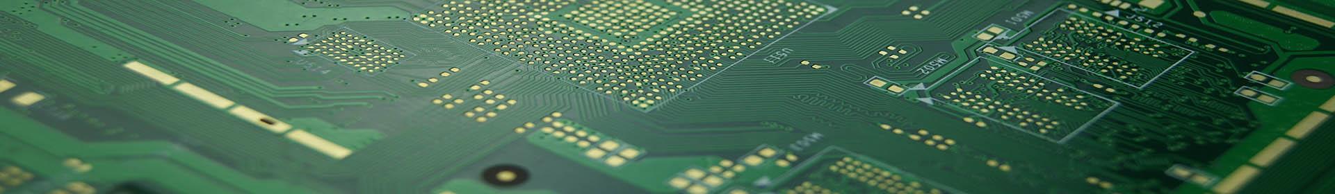
Thermal Simulation and Conductor Cross-Sectional Area Comparison Between Standard and Thick Copper PCBs Under High-Current Load
Heavy copper layers alter the PCB thermal network by minimizing vertical thermal resistance (RθJC) and establishing massive planar heat dissipation paths, while structurally reinforcing high-stress component junctions such as heavy-gauge wire terminals and busbars[cite: 19].
Thermal Scaling and IPC-2152 Validation
Relying on the IPC-2152 standard for current carrying capacity, a 30°C temperature rise (ΔT) for an internal trace carrying 80A requires a cross-sectional area of approximately 1,200 mil2 with 1 oz copper, dictating an unfeasible trace width of 12 inches[cite: 21]. Transitioning to a 5 oz (175 µm) copper layer reduces the required trace width to just 1.71 inches, reclaiming 85.7% of board real estate for dense component placement.
Parameterized Trace Width and Thermal Conductivity Matrix
| Copper Thickness (oz / µm) |
Required Trace Width (for 60A load @ ΔT = 20°C) |
DC Resistance per Inch (Width = 500 mil) |
Thermal Conductivity Matrix (W/m·K) |
|---|---|---|---|
| 1 oz / 35 µm | 5.40 inches (137.1 mm) | 0.98 mΩ | Conductor: 398 | Base FR4: 0.25 |
| 3 oz / 105 µm | 1.80 inches (45.7 mm) | 0.32 mΩ | Enhanced Lateral Spreading: Effective Layer K ∼ 45 |
| 5 oz / 175 µm | 1.08 inches (27.4 mm) | 0.19 mΩ | Highly Integrated Thermal Core: Effective Layer K ∼ 85 |
| 10 oz / 350 µm | 0.54 inches (13.7 mm) | 0.09 mΩ | Extreme Metal Base Spreading: Effective Layer K ∼ 160 |
Mechanical Integration of High-Current Fasteners
Heavy-duty power supplies utilize threaded M5 studs or heavy copper busbars soldered directly to the board[cite: 25]. Standard PCB pads peel off under the mechanical rotational torque (typically 2.5 N-m) or fail during thermal cycling due to Coefficient of Thermal Expansion (CTE) mismatch between the FR4 resin and the brass terminal[cite: 26]. Thick copper traces feature high peel strength (>10 lb/in compared to 6 lb/in for standard copper), guaranteeing structural longevity under vibration profiles specified by automotive testing frameworks like LV124.
3. Design for Manufacturing (DFM) Metrics for Layout Optimization
Thick copper layouts require strict modification of trace-to-trace spacing, minimum line widths, pad annular rings, and solder mask clearance rules due to the physical realities of lateral chemical etching and high-viscosity resin flow during lamination[cite: 31]. When copper exceeds 3 oz, a standard 1:1 etch factor is completely unachievable because chemical etchants work downwards and outwards simultaneously[cite: 32]. For a 4 oz (140 µm) trace, the lateral undercut (side etching) can range from 35 µm to 50 µm per side.
Parameterized DFM Rule-Matrix
- Minimum Trace Width / Spacing: For 3 oz copper, the absolute minimum line/space is 10/12 mils (0.25/0.30 mm)[cite: 35]. For 6 oz copper, this scales strictly to 18/22 mils (0.45/0.55 mm) to prevent micro-bridging.
- Annular Ring Constraints: Via pads must expand[cite: 37]. A 4 oz copper layer requires an outer layer annular ring of at least 12 mils (0.30 mm) per side to compensate for drill drift and etch back without causing breakout.
- Thermal Relief Pads: Direct connection of a solid 4 oz plane to component pins acts as a massive thermal sink during assembly, freezing solder paste[cite: 38]. A 4-way thermal relief pad with a minimum spoke width of 20 mils (0.50 mm) is mandatory to ensure reliable wetting.
Critical Engineering Pain Point: Lamination Resin Voiding & Micro-Cavitations
In multi-layer boards featuring internal 4 oz power planes adjacent to 1 oz signal planes, the 140 µm step height creates massive geometric topography[cite: 41]. Standard Prepreg (e.g., 7628 or 2116) lacks the fluid volume to completely fill the wide "canyons" between dense thick copper traces during the lamination press cycle[cite: 42]. This results in microscopic air entrapped bubbles (voids)[cite: 43]. Under 400V+ operational conditions typical of EV traction inverters, these localized air cavities undergo partial discharge, degrading the dielectric material over time and culminating in catastrophic, low-impedance Z-axis shorts.
"At Hongda Circuit, we address this by mandating a High-Resin Content (HRC) prepreg stackup combination (e.g., combining 1080 high-resin content with 7628 structured glass) and applying a customized vacuum hydraulic press curve. We extend the vacuum dwell time from 20 minutes to 45 minutes at 130°C before ramping to the full 185°C curing phase, ensuring perfect polymer fluidization and 100% void-free encapsulation." — Manufacturing Engineering Fix, Shenzhen Hongda Circuit Technology Co., Ltd. .
4. Manufacturing Bottlenecks and Processing Breakthroughs
The main manufacturing bottlenecks include severe photoresist breakdown under prolonged chemical etching, solder mask skipping over steep trace walls, and extreme thermal inertia during automated optical inspection (AOI) and chemical plating steps.
Lithography and Etch Factor Correction
Standard liquid photoresist fails on thick copper because the coating thins out at the sharp 90-degree top corners of the trace, leading to pinholes and trace nicking during acid spray exposure[cite: 51]. To bypass this limitation, we deploy a dual-stage dry-film lamination process, combining a conformable 2.0-mil (50 µm) thick photoresist applied under high-pressure wet-lamination parameters[cite: 52]. The artwork pattern is artificially compensated in the CAM station using a proprietary non-linear scaling matrix.
Solder Mask Application over Steep Profiles
A standard curtain coater or single-pass screen print cannot deposit adequate ink onto the vertical sidewalls of a 5 oz trace without leaving a thick puddle at the base, which remains uncured and traps moisture[cite: 57]. To resolve this, we employ a double-shuttle electrostatic spray coating system, followed by an intermediate tack-dry cycle and a secondary vertical screen printing pass[cite: 58]. This guarantees a minimum insulation thickness of 18 µm on the trace crown and 15 µm along the 90-degree vertical flanks.
"When drilling through a multi-layer board with internal 6 oz copper cores, standard feed and speed rates will shatter the carbide bit within fifty hits. The drill tip encounters massive thermal shock as it crosses from ductile copper to abrasive fiberglass. We had to rewrite our CNC parameters entirely—dropping the spindle speed by 35% and increasing chip load per revolution while utilizing water-cooled aluminum entry sheets." — Drilling Department Superintendent, Shenzhen Hongda Circuit Technology Co., Ltd.
5. Power Electronics Real-World Scenarios
 details a 4-layer server power supply lamination stack-up with 4 oz heavy copper inner layers and filled thermal vias, showing the direct heat transfer pathway from a surface-mounted MOSFET to reduce thermal resistance. Scene B (right) contrasts a conventional power loop against an advanced interleaved power loop topology utilizing 6 oz heavy copper for an EV traction inverter, complete with circuit schematics and voltage waveform graphs demonstrating a reduction of loop inductance below 4.5 nH and the suppression of SiC voltage spikes.")
Application Architecture Scenarios for Heavy Copper PCBs in 3KW Server PSUs (Scene A) and 800V SiC EV Traction Inverters (Scene B).
Real-world high-power scenarios require thick copper to mitigate localized hot spots in restricted-airflow chambers, bridge high-voltage isolation boundaries, and support ultra-low loop inductance paths for high-frequency switching cells.
-
Scenario A: 3KW Server Telecommunications Rectifier (48V Output Architecture)
In cloud data center power bricks, space is limited to a standard 1U rack profile (44 mm height limit)[cite: 67]. The secondary output stage delivers up to 62.5A continuous at 48VDC[cite: 68]. To eliminate massive mechanical copper busbars that block airflow, the design embeds a 4-layer PCB with 4 oz internal copper layers[cite: 69]. The synchronous rectification MOSFETs (DirectFET or LFPAK packages) are soldered directly onto large 4 oz solid copper planes[cite: 70]. This setup drops trace operating temperatures from 115°C down to 78°C without requiring dedicated chassis-mounted heat sinks, successfully satisfying Energy Star Gen 3 efficiency mandates. -
Scenario B: 800V Silicon Carbide (SiC) EV Traction Inverter
Next-generation EV inverters operate at 800V DC-link voltages with dV/dt switching transients exceeding 50 V/ns[cite: 73]. Any stray trace inductance generates severe voltage spikes (V = L × di/dt) that can puncture the SiC MOSFET gate oxide[cite: 74]. By implementing a 6 oz multi-layer interleaved power structure, we reduce trace thickness-to-width ratios, compressing the loop inductance to less than 4.5 nH[cite: 75]. Furthermore, the massive copper weight provides a high thermal capacitance matrix, absorbing transient energy overloads during peak regenerative braking events (up to 250A for 10 seconds).
6. Frequently Asked Questions & Parametric Comparisons (FAQ)
Standard 1 oz copper requires a minimum trace clearance of 4 to 5 mils[cite: 94]. As copper thickness scales, DFM rules scale up linearly to account for lateral undercut: 3 oz requires a minimum spacing of 12 mils (0.30 mm); 5 oz requires 16 mils (0.40 mm); and ultra-thick 8 oz copper dictates a minimum isolation clearance of 24 mils (0.60 mm) to ensure complete chemical extraction of unexposed copper elements within the etch chamber.
About Author
David Chen https://www.linkedin.com/in/pcbcomingDavid Chen boasts an extensive professional background in PCBA manufacturing, PCBA testing, and PCBA optimization, with specialized expertise in high-precision PCBA fault analysis and rigorous PCBA reliability testing. The author has worked with high-layer-count server PCB fabrication, ultra-low-loss backplane stackups, and thermo-mechanical reliability optimization for AI infrastructure projects involving 112G and 224G PAM4 architectures. Skilled in complex circuit design and cutting-edge advanced PCB manufacturing processes, he delivers solutions that elevate product durability and performance across industrial applications. His technical articles focusing on PCBA manufacturing workflows and testing methodologies are widely cited by industry peers, research institutions, and technical platforms, solidifying his reputation as a recognized technical authority in the global circuit board manufacturing sector.