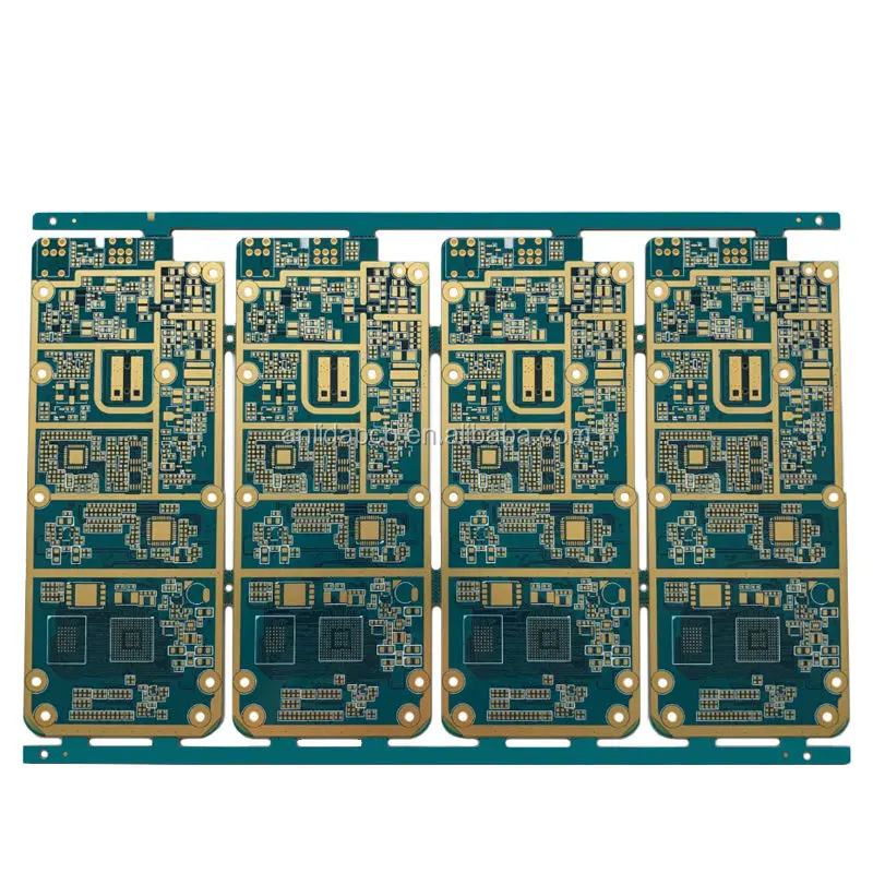
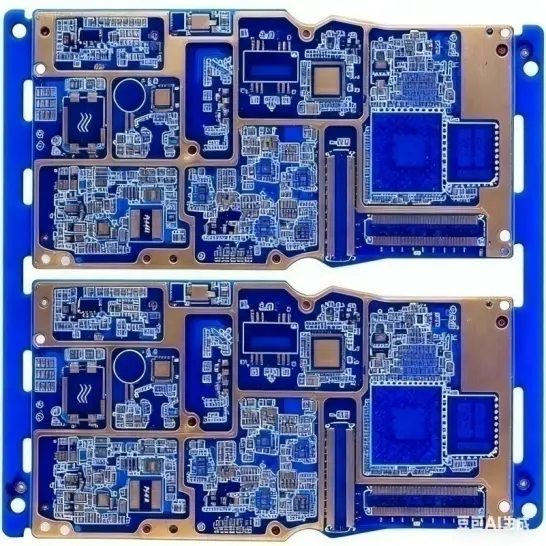
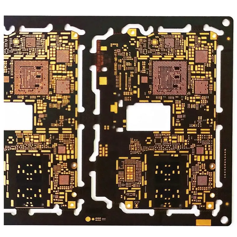
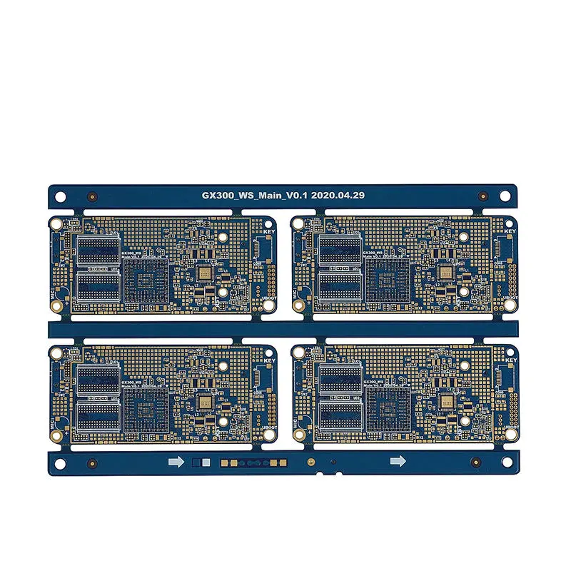
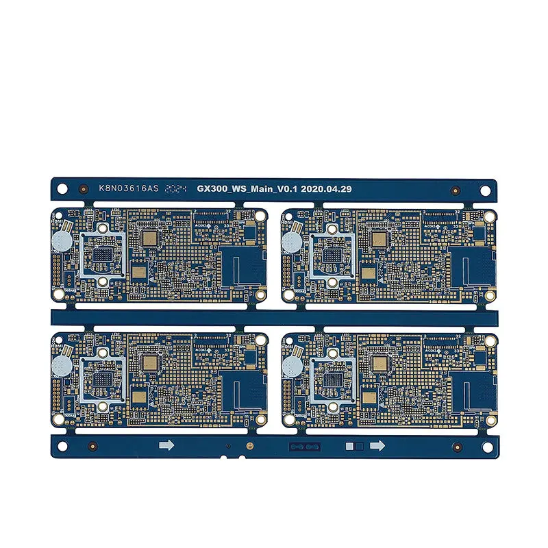
Technical Overview of a 6-Layer 1+N+1 HDI PCB for Mobile Phone Applications
The demand for compact, high-performance mobile devices continues to drive innovation in printed circuit board (PCB) technology. A 6-layer 1+N+1 stack-up represents a sophisticated HDI (High-Density Interconnect) solution commonly employed in modern smartphone motherboards. This article provides a detailed technical examination of the specifications for such a PCB, highlighting key manufacturing considerations.
1. Core Material and Construction
"The foundation of this PCB is a high-performance S1000-2 high-Tg (Glass Transition Temperature) material. This halogen-free laminate is engineered for superior thermal reliability, resisting deformation and maintaining structural integrity during the high-temperature soldering processes typical in surface-mount technology (SMT) assembly. This is critical for ensuring long-term reliability in consumer electronics.
The board features a 6-layer 1+N+1 HDI build-up. This configuration signifies one sequential lamination cycle: a core layer (N) is sandwiched between layers of microvias, allowing for higher routing density in a thinner board. The final finished thickness is precisely controlled at 0.8mm, striking a balance between mechanical rigidity and the slim profile required for mobile phones."
2. Copper Distribution and Circuit Density
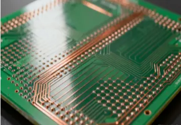
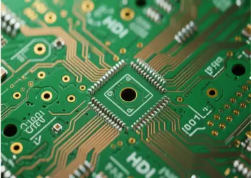
differentiated copper weight strategy is implemented: 1 oz (approximately 35 µm) on the outer layers and 0.5 oz (approximately 17.5 µm) on the inner layers. This configuration provides robust current-carrying capacity and enhanced thermal dissipation on the surface for components, while the thinner inner layers facilitate the etching of finer traces within the dense internal signal layers.
The design supports a minimum trace width and spacing of 3 mil (mil/1000th of an inch, approximately 76.2 µm). This 3/3 mil capability is a hallmark of HDI technology, enabling the complex routing necessary for high-pin-count components like application processors, memory, and modern chipsets.
3. Advanced Surface Finish and Solderability
A combination surface finish of Electroless Nickel Immersion Gold (ENIG) and Organic Solderability Preservative (OSP) is specified. The ENIG finish on the gold fingers provides a hard, flat, and oxidation-resistant contact surface, ideal for connectors. The OSP coating on other areas protects the copper pads from oxidation before soldering, offering a cost-effective and planar surface for fine-pitch component placement. This hybrid approach optimizes both performance and manufacturability.
4. Application and Conclusion
This combination of specifications—specifically the HDI stack-up, fine line technology, and advanced materials—makes this PCB ideally suited for the mainboard of advanced mobile phones. It provides the necessary electrical performance, signal integrity, and miniaturization required by today's compact, feature-rich devices.
In summary, this set of technical specifications outlines a robust manufacturing framework for a high-density mobile phone PCB. The use of S1000-2 material, a 1+N+1 layer build-up, 3/3 mil design rules, and a hybrid ENIG+OSP surface treatment collectively define a PCB capable of meeting the rigorous demands of contemporary mobile electronics.
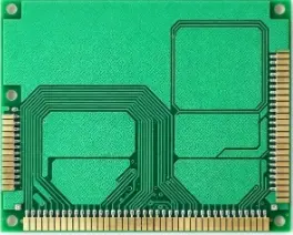
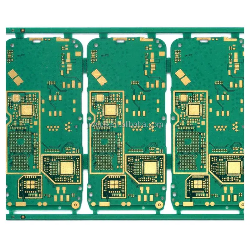
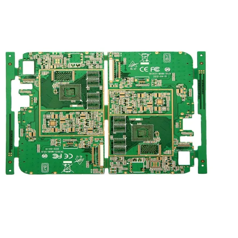
Product Model: 6-Layer 1+N+1 Mobile Phone PCB
Base Material: High-Tg Material S1000-2
Layer Construction: 6-Layer, 1+N+1 Stack-up
Solder Mask Color: Green / White
Finished Board Thickness: 0.8 mm
Copper Weight: Inner Layers: 0.5 oz, Outer Layers: 1 oz
Surface Finish: ENIG (Electroless Nickel Immersion Gold) + OSP (Organic Solderability Preservative)
Minimum Line Width / Spacing: 3 mil / 3 mil
Primary Application: High-Density Interconnect (HDI) Mobile Phone PCB