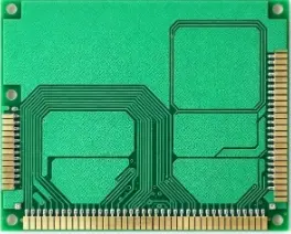
Technical Deep Dive: An 8-Layer HDI 2+N+2 Mobile Main Board for Next-Generation Devices
The demand for more compact, powerful, and feature-rich mobile devices relentlessly drives innovation in printed circuit board (PCB) technology. At the heart of this evolution lies the High-Density Interconnect (HDI) PCB. This article provides a technical analysis of a sophisticated 8-Layer HDI Mobile Main Board utilizing an advanced 2+N+2 build-up construction, engineered to meet the stringent requirements of modern mobile applications.
Core Architecture: 2+4+2 HDI Stack-Up
"The fundamental architecture of this board is defined by its 2+4+2 HDI construction. This terminology specifies a sequential build-up process:
1、The core of the board is a standard 4-layer PCB (the ""N"" layer).
2、This core is then laminated with additional dielectric and copper foil on both sides.
3、Two sequential HDI layers are built up on the top and bottom, connected by microvias."
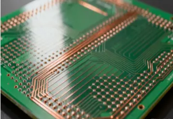
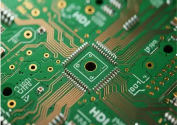
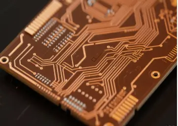
This structure allows for a significantly higher wiring density than conventional PCBs. The use of microvias—laser-drilled holes with a diameter of 0.1mm—enables direct, short interconnections between layers, reducing signal path length and improving electrical performance, which is critical for high-speed signals found in mobile processors and RF components.
Critical Material and Fabrication Specifications
"The selection of materials and fabrication tolerances is paramount to the board's reliability and performance:
1、Base Material: The board utilizes TG170 FR4 laminate. This indicates a glass transition temperature (Tg) of 170°C, providing enhanced thermal stability and resistance against thermal stress during lead-free soldering processes, a standard in modern electronics manufacturing.
2、Finished Thickness: The board is engineered to an ultra-thin 0.8mm finished thickness. This slim profile is essential for the sleek form factors demanded by today's smartphones and portable devices.
3、Copper Thickness: A 0.5-ounce (OZ) copper weight is used for the signal layers. This standard weight offers an optimal balance between current-carrying capacity and the ability to etch fine-line features.
4、Fine-Line Fabrication: The board supports a minimum trace width and spacing of 3 mil (0.075mm). This ultra-fine line capability is a hallmark of HDI technology, allowing for a greater number of circuits in a confined area.
5、Surface Finish: The board features a combination of Immersion Gold (ENIG) over an OSP (Organic Solderability Preservative). This hybrid finish provides a flat, gold-plated contact surface for reliable component soldering and a protective OSP coating on the remaining copper to prevent oxidation."
Application and Advantages
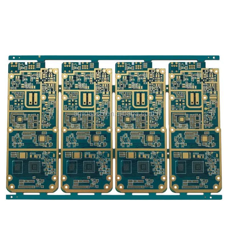
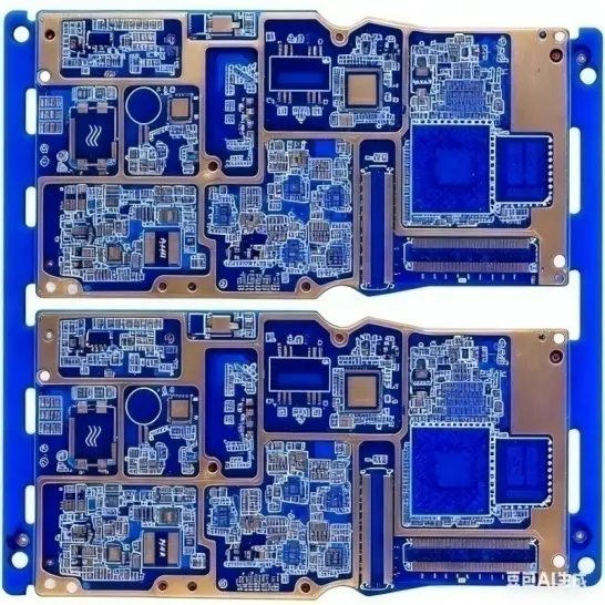
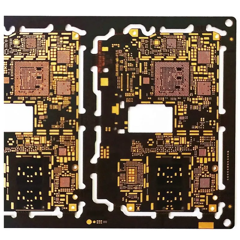
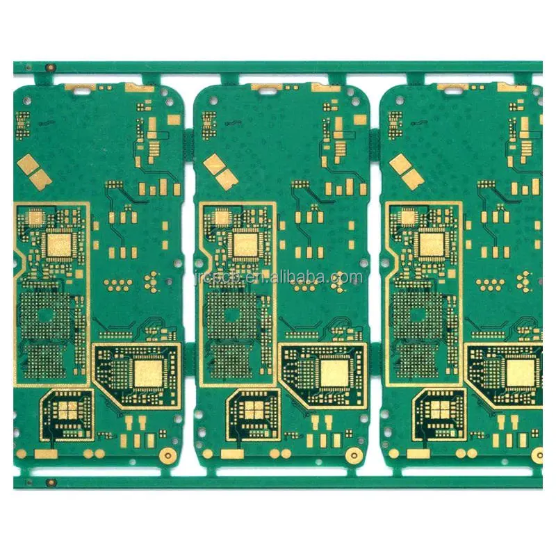
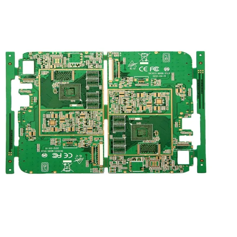
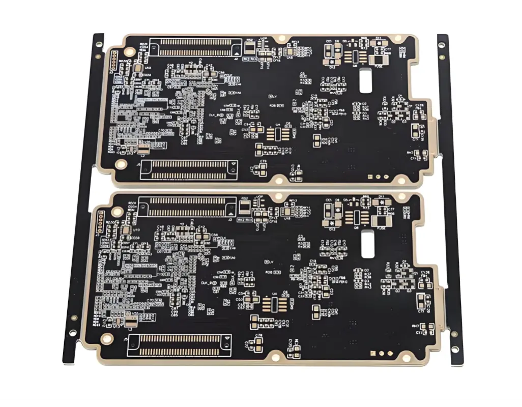
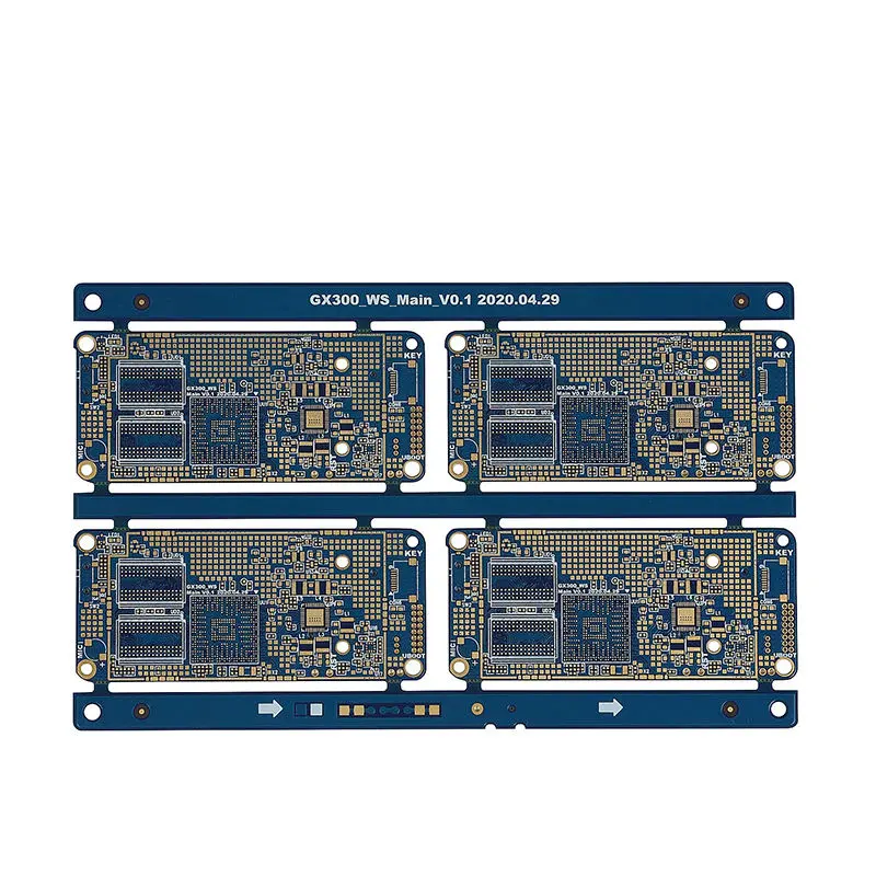
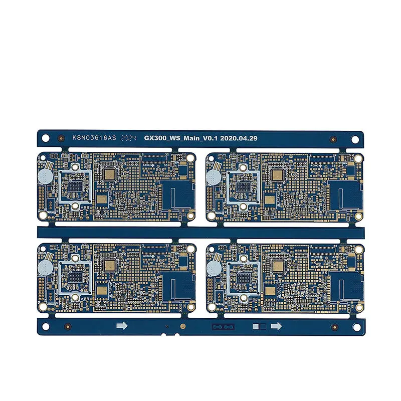
"This 8-Layer HDI PCB is specifically designed as a Mobile Main Board. Its primary advantages include:
1、Space Efficiency: The high wiring density allows for a more compact board design, freeing up valuable internal space for larger batteries or additional components.
2、Enhanced Signal Integrity: Shorter signal paths and reduced parasitic effects from microvias contribute to cleaner signal transmission at high frequencies.
3、Improved Reliability: The robust TG170 material and sophisticated construction enhance the board's durability under mechanical and thermal stress."
In summary, this 8-layer HDI PCB with its 2+N+2 construction represents a peak of modern circuit board manufacturing for the mobile industry. By leveraging advanced materials like TG170 FR4 and pushing fabrication limits with 3/3 mil trace/space and 0.1mm laser microvias, it provides the essential foundation for developing the next generation of high-performance, compact mobile devices. Engineers seeking a reliable and high-density solution for space-constrained applications will find this technology indispensable.
Model: 2+N+2 Mobile Main Board
Layer Count: 8 Layers
Base Material: TG170 FR-4
PCB Construction: 2+4+2 HDI Stackup
Board Thickness: 0.8 mm (Finished)
Copper Weight: 0.5 oz
Solder Mask: Green/White
Surface Finish: ENIG with OSP (Immersion Gold + Organic Solderability Preservative)
Minimum Trace/Space: 3 mil / 3 mil
Minimum Via Size: 0.1 mm Laser-drilled Micro-via
Application: Mobile Main Board